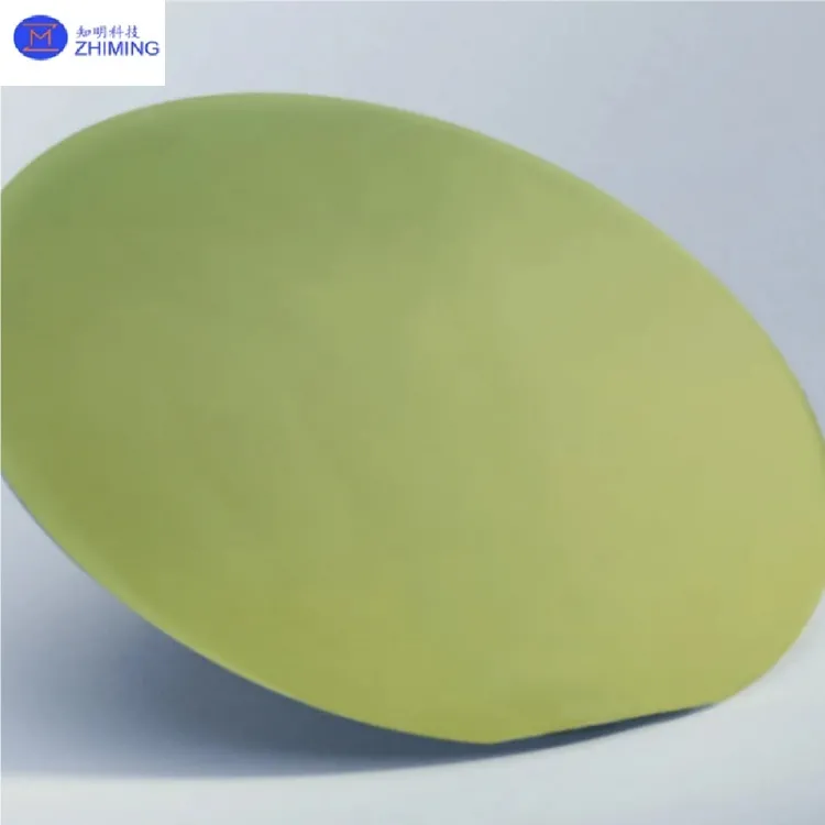
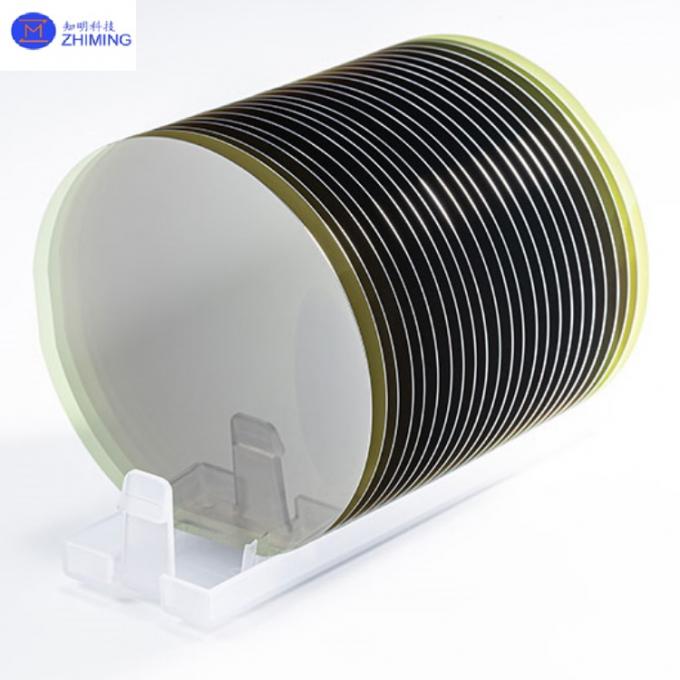
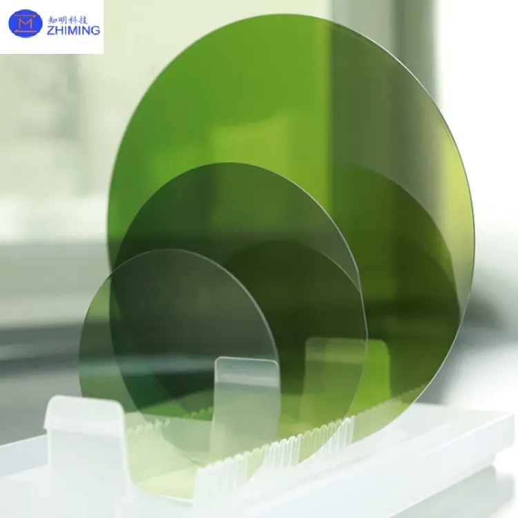
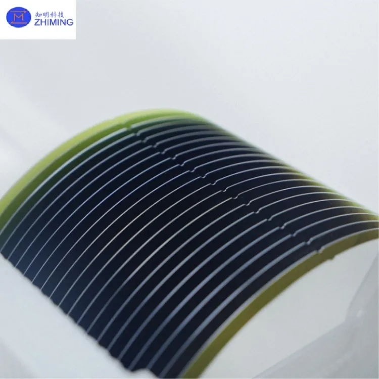
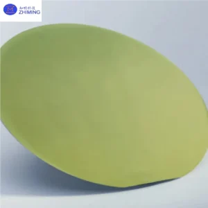
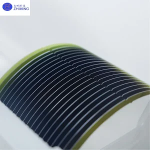
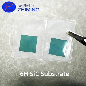
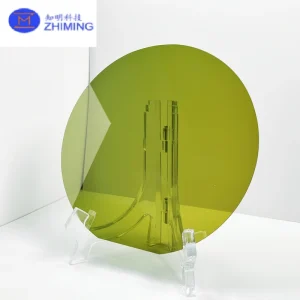
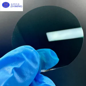
 The 8 inch (200mm) 4H-N Silicon Carbide epitaxial wafer is designed for next-generation high-power and high-frequency electronic devices. Built on high-purity SiC substrates and grown using advanced Chemical Vapor Deposition (CVD) technology, this product offers excellent uniformity, low defect density, and high electrical performance.
It is widely used in electric vehicles, renewable energy systems, industrial power electronics, and RF applications.
Key Features
Large Diameter for Cost Efficiency
The 200mm wafer provides approximately 78 percent more usable area compared to traditional 150mm wafers. This significantly improves chip output per wafer and reduces overall device cost by around 30 percent. It is well suited for large-scale automated manufacturing.
Ultra-Low Defect Density
Surface defect density is controlled to less than or equal to 0.5 per square centimeter. Basal plane dislocation conversion efficiency exceeds 99 percent, ensuring high device yield and long-term reliability in high-voltage applications.
Precise Epitaxial Growth
Using advanced CVD processes, the epitaxial layer achieves thickness uniformity within 3 percent and doping uniformity within 5 percent. Background carrier concentration is maintained below 1×10¹⁴ cm⁻³, supporting stable device characteristics.
High Electrical Performance
The wafer supports a breakdown electric field greater than or equal to 3 MV/cm and electron mobility above 1000 cm²/V·s. It is suitable for device voltage ranges from 650V to 3300V.
High Reliability and Stability
The product meets automotive-grade reliability requirements. Under high temperature reverse bias testing at 175°C for 1000 hours, parameter drift remains within 0.5 percent. It also demonstrates strong environmental stability under high humidity conditions.


Technical Specifications
| Parameter | Specification |
|---|---|
| Diameter | 200 mm |
| Thickness | 500 ±25 μm |
| Epitaxial Thickness | 5–20 μm (customizable) |
| Thickness Uniformity | ≤3% |
| Doping Uniformity | ≤5% |
| Surface Defect Density | ≤0.5/cm² |
| Surface Roughness | ≤0.5 nm |
| Electron Mobility | ≥1000 cm²/V·s |
| Breakdown Field | ≥3 MV/cm |
| Carrier Concentration | 5×10¹³ – 1×10¹⁹ cm⁻³ |
| Crystal Structure | 4H-SiC (off-axis ≤0.5°) |
| Supported Devices | MOSFET, SBD, JBS, IGBT |
Applications
Electric Vehicles
Used in traction inverters and onboard chargers, supporting high-voltage platforms such as 800V systems and enabling fast charging and high efficiency.
Renewable Energy Systems
Applied in solar inverters and energy storage converters, improving system efficiency and reducing energy loss.
Industrial Power Electronics
Suitable for power factor correction modules and high-frequency converters, enabling higher switching frequencies and increased power density.
RF and 5G Devices
Used as substrates for GaN-based RF devices, improving power amplifier efficiency and signal performance.
Customization Options
Custom epitaxial structures are available upon request, including:
- Epitaxial layer thickness adjustment
- Doping concentration control
- N-type or semi-insulating structures
Frequently Asked Questions
What are the advantages of 8 inch SiC epitaxial wafers compared to 6 inch wafers?
The 8 inch wafer offers significantly higher usable area, improving chip output and reducing cost per device. It also aligns better with modern automated fabrication processes.
Can the epitaxial structure be customized?
Yes, epitaxial thickness, doping concentration, and layer structure can be tailored according to device requirements.
How is quality ensured?
Each wafer undergoes strict inspection for surface defects, thickness uniformity, and doping consistency. Reliability testing such as high temperature reverse bias testing is also performed.
What industries is this product best suited for?
This product is ideal for electric vehicles, renewable energy systems, industrial power electronics, and RF communication applications.
Reviews
There are no reviews yet.