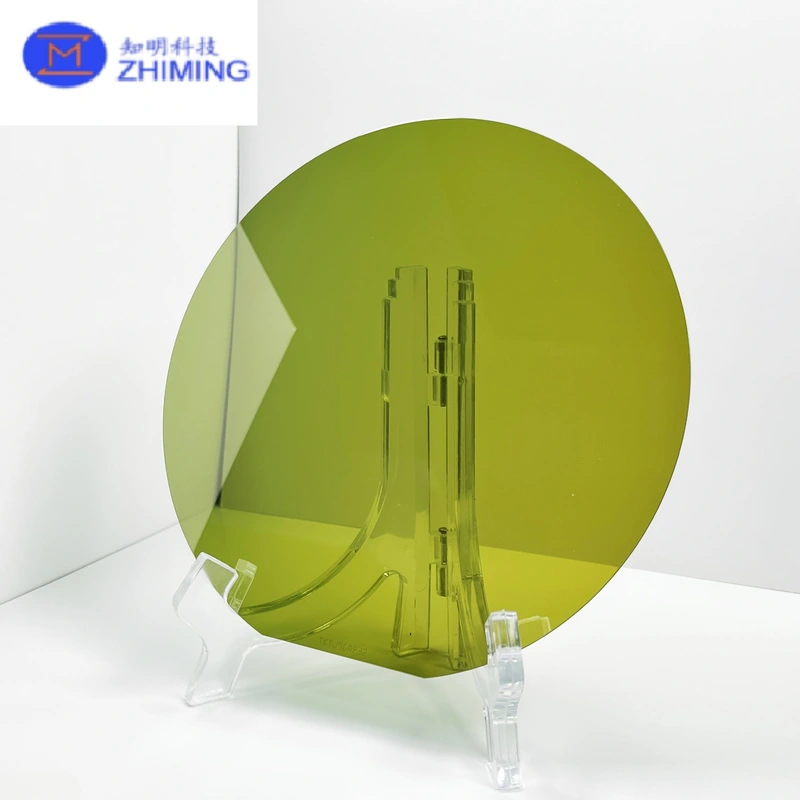
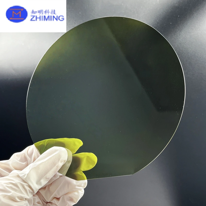

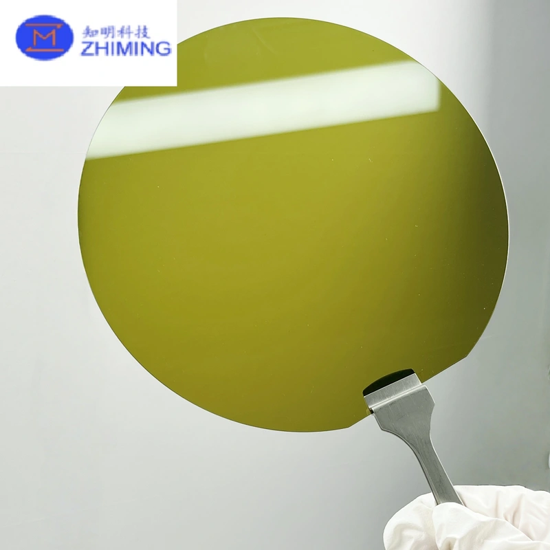
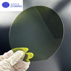
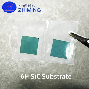
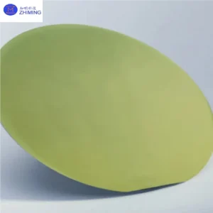
 The 4H-N type and Semi-Insulating (SI) Silicon Carbide (SiC) substrates are high-performance single-crystal wafers engineered for next-generation power electronics, RF devices, and epitaxial applications. Manufactured using the advanced Physical Vapor Transport (PVT) method, these substrates offer exceptional material purity (≥99.9995%), low defect density, and superior structural consistency.
As a representative material of wide bandgap semiconductors, 4H-SiC delivers outstanding high-voltage tolerance, high-frequency performance, and thermal stability, making it an essential platform for modern semiconductor devices.
- 4H-N type substrates are optimized for power device fabrication such as MOSFETs and Schottky diodes
- Semi-insulating substrates are ideal for RF and microwave applications, including GaN epitaxy and high-frequency circuits
Key Features
1. Superior Electrical Performance
- 4H-N Type Resistivity: 0.015–0.028 Ω·cm
- Semi-Insulating Resistivity: ≥10⁵ Ω·cm
- Wide bandgap (~3.26 eV) supports high breakdown voltage (3–5 MV/cm)
- Enables low switching loss and high efficiency in power devices
2. Excellent Thermal & Mechanical Properties
- Thermal conductivity up to ~4.5 W/cm·K
- Operates reliably in temperatures above 600°C
- High hardness (~Mohs 9.2), ensuring durability during processing
3. High-Precision Geometric Control
- Total Thickness Variation (TTV): ≤ 15 µm
- Bow: ≤ 25 µm
- Warp: ≤ 5 µm
- Ensures excellent compatibility with epitaxial growth and lithography processes
4. Controlled Crystal Orientation
- On-axis orientation: < ±0.5°
- Off-axis orientation: 4° ±0.5° toward <11-20>
- Optimized for epitaxial layer uniformity and defect suppression
5. Advanced Surface Quality
- Standard polished surface: Ra ≤ 1 nm
- CMP surface: Ra ≤ 0.5 nm (epi-ready)
- Low micropipe density:
- Zero-grade: ≤ 1 cm⁻²
- Production-grade: ≤ 5 cm⁻²
Applications
Power Electronics
- SiC MOSFETs
- Schottky Barrier Diodes (SBD)
- IGBTs
Widely used in electric vehicles, industrial inverters, and energy systems
RF & Microwave Devices
- High-frequency amplifiers
- MMICs (Monolithic Microwave Integrated Circuits)
- Especially suited for 5G, radar, and satellite communications
Optoelectronics
- GaN-based LEDs and laser diodes
- UV photonic devices
High-Temperature & Harsh Environments
- Aerospace electronics
- Automotive sensors
- Energy and oil & gas applications
Manufacturing Process Highlights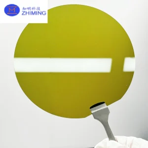
- PVT Crystal Growth: Ensures high-purity and stable 4H polytype
- Diamond Wire Slicing: Precision wafer thickness control
- Lapping & Grinding: Improves flatness and removes subsurface damage
- CMP Polishing: Produces ultra-smooth epi-ready surfaces
- Strict Quality Inspection: Includes resistivity mapping, defect density, and geometry verification
Technical Specifications
| Parameter | Specification |
|---|---|
| Material | SiC Single Crystal |
| Type | 4H-N / Semi-Insulating |
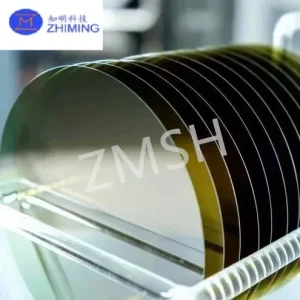
| Diameter | 2, 3, 4, 6, 8 inch |
| Purity | ≥ 99.9995% |
| Resistivity | N-type: 0.015–0.028 Ω·cm / SI: ≥10⁵ Ω·cm |
| Thickness | 330–500 µm (customizable) |
| TTV | ≤ 15 µm |
| Bow | ≤ 25 µm |
| Warp | ≤ 5 µm |
| Surface Roughness | Ra ≤ 0.5 nm (CMP) |
| Orientation | On-axis / 4° off-axis |
| Packaging | Single wafer box / 25pcs cassette |
 Customization Options
We offer full customization to meet different device and process requirements:
- Wafer size: 2″ to 8″
- Thickness adjustment
- Orientation control (on-axis / off-axis)
- Surface finish (DSP / CMP / epi-ready)
- Resistivity & doping tuning
- Special coatings or epitaxial services
Industry Value
In the SiC industry chain, substrates form the foundation of device performance. High-quality substrates directly determine epitaxial layer quality, device yield, and long-term reliability.
Our 4H-SiC wafers are widely used as base materials for epitaxial growth (CVD) and advanced device fabrication, supporting the rapid development of EVs, renewable energy systems, and high-frequency communication technologies.
FAQs
Q1: What is the difference between 4H-N and Semi-Insulating SiC?
A: 4H-N is conductive and used for power devices, while semi-insulating SiC is used for RF and microwave applications due to its high resistivity.
Q2: Are the wafers epi-ready?
A: Yes, CMP-polished wafers are epi-ready and suitable for direct epitaxial growth.
Q3: Can I customize specifications?
A: Yes, we support full customization including size, thickness, resistivity, and orientation.
Q4: What quality documents are provided?
A: Each wafer comes with a test report, including resistivity mapping, TTV, and defect inspection data.
Reviews
There are no reviews yet.