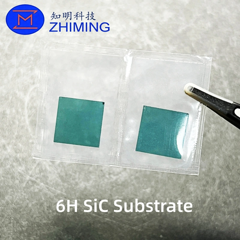
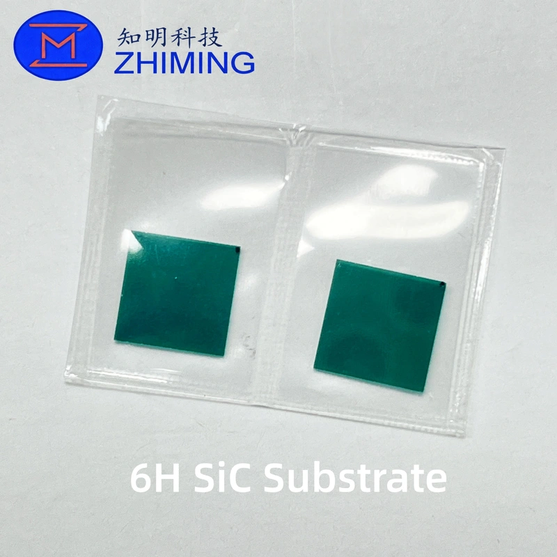
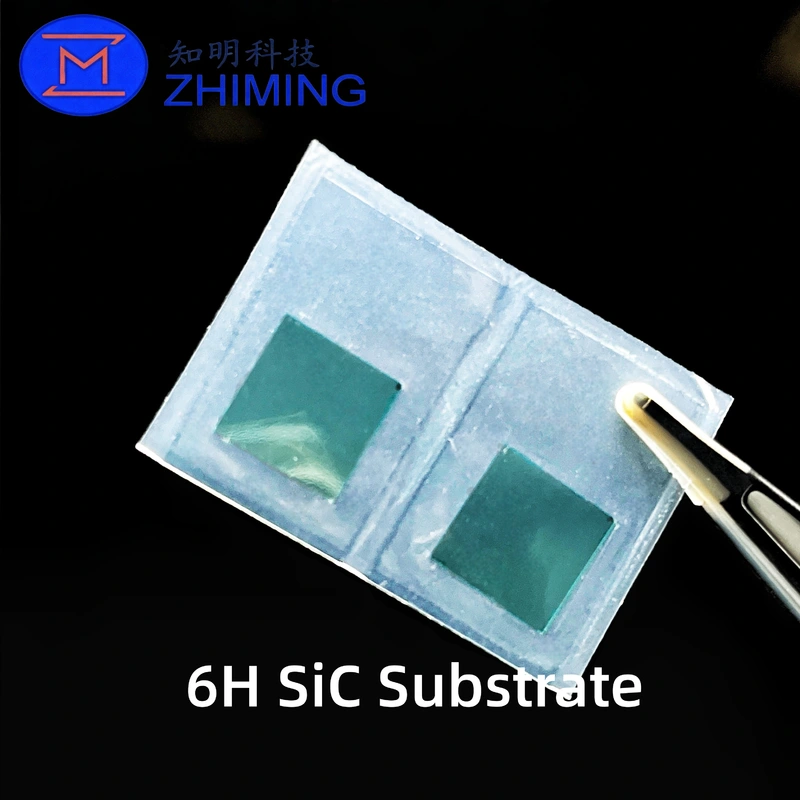
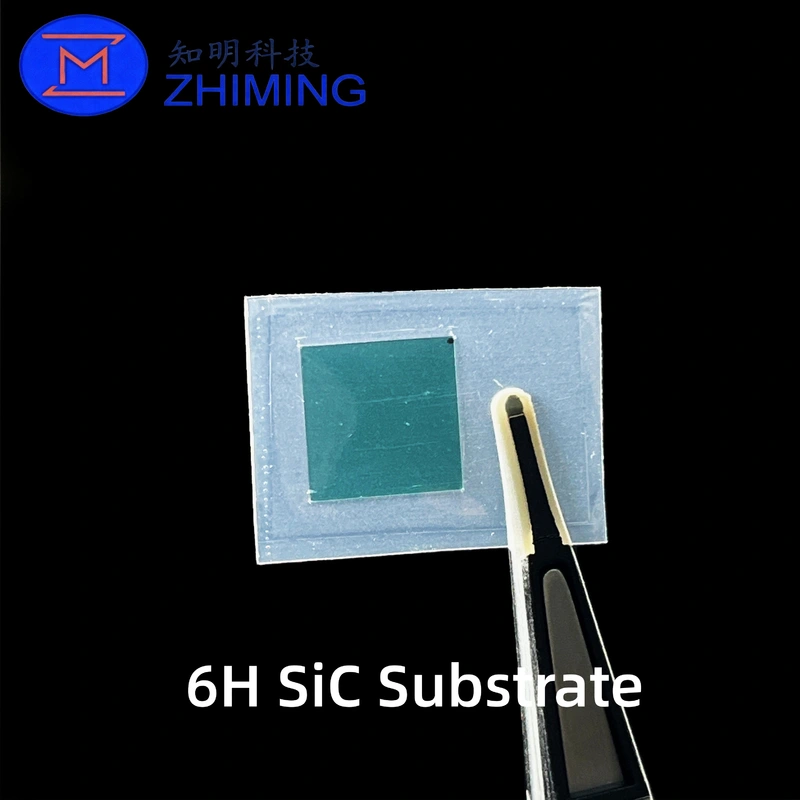
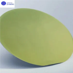
 6H Silicon Carbide (SiC) substrates are single-crystal wafers engineered for high-temperature, high-voltage, and specialized optoelectronic applications. Featuring a stable hexagonal crystal structure, 6H SiC offers excellent thermal conductivity, mechanical strength, and chemical resistance.
Compared to 4H SiC, 6H SiC provides a cost-effective solution for applications where extreme thermal stability, UV response, and material robustness are more critical than high electron mobility. It is widely used in UV optoelectronics, high-temperature sensors, and industrial electronics.
Key Features
Stable 6H Crystal Structure
The hexagonal 6H polytype provides strong lattice stability and mechanical integrity, ensuring consistent performance during wafer processing and device fabrication.
High Thermal Conductivity
With thermal conductivity in the range of 390 to 450 W/m·K, the substrate enables efficient heat dissipation in high-temperature and high-power environments.
Excellent Mechanical and Chemical Stability
High hardness and corrosion resistance make 6H SiC suitable for harsh environments, including aerospace, automotive, and industrial systems.
Flexible Electrical Properties
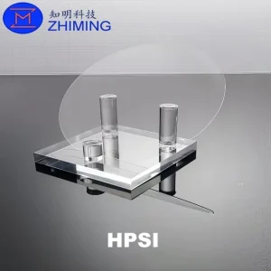
Available in both N-type conductive and semi-insulating (SI) forms, supporting a wide range of applications from power devices to RF and microwave circuits.
Epitaxy-Compatible Surface
Epi-ready surfaces are available through CMP and hydrogen annealing processes, ensuring compatibility with epitaxial growth and advanced device structures.
Wide Size and Customization Range
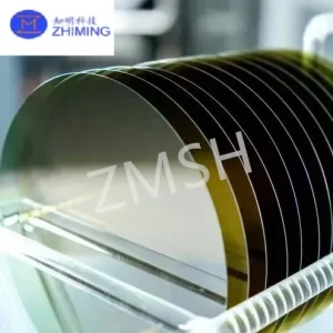
Available in diameters from 2 inch to 12 inch, as well as square or custom geometries. Thickness and surface finish can be tailored to specific requirements.
Technical Specifications
| Parameter | Specification |
|---|---|
| Material | Single-Crystal 6H SiC |
| Crystal Structure | Hexagonal (6H) |
| Diameter / Size | 2″, 4″, 6″, 8″, 12″ (25–300 mm), square or custom sizes available |
| Thickness | 350–1000 µm (customizable) |
| Surface Finish | Epi-ready CMP, DSP, SSP |
| Total Thickness Variation (TTV) | ≤5 µm (typical) |
| Bow / Warp | ≤40 µm (6 inch typical) |
| Micropipe Density | <0.1 cm⁻² (industrial), <0.01 cm⁻² (premium) |
| Dislocation Density | <10⁴ cm⁻² |
| Thermal Conductivity | 390–450 W/m·K |
| Conductivity Type | N-type or Semi-Insulating |
| Epitaxy Compatibility | Yes |
Application Areas
High-Temperature Electronics
Used in sensors and electronic systems operating in extreme thermal environments where silicon-based materials fail.
UV Optoelectronics
Suitable for UV LEDs and photodetectors due to its wide bandgap and optical properties.
Aerospace and Automotive Systems
Provides stable performance in high-radiation, high-temperature, and high-vibration conditions.
Industrial Power and Control Systems
Enables compact, durable designs for power modules and control electronics.
RF and Microwave Devices
Semi-insulating 6H SiC substrates reduce signal loss and improve performance in high-frequency circuits.
Research and Development
Widely used in material science and wide bandgap semiconductor research.
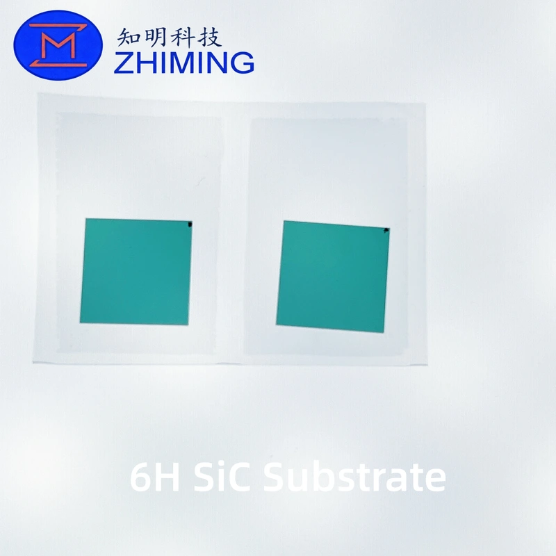
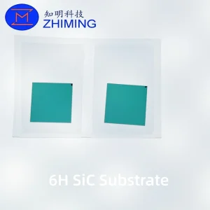
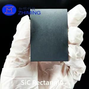
Square Substrate Advantages
Square SiC substrates offer improved material utilization and alignment efficiency in certain applications:
- Better electrode alignment for sensors and optoelectronic devices
- Reduced packaging gaps in compact modules
- Improved layout efficiency for RF and microwave circuits
 Manufacturing Process
The production of 6H SiC substrates follows a high-precision process:
- High-purity SiC powder synthesis
- Seed crystal mounting for controlled growth
- High-temperature sublimation growth at 2300–2500°C
- Diamond wire slicing into wafers
- Precision polishing using CMP or diamond techniques
- Full inspection and quality certification (CoA available)
 Customization Options
We support flexible customization based on application requirements:
- Diameter and geometry (round or square)
- Thickness adjustment
- Surface finish (CMP, DSP, SSP)
- Conductivity type (N-type or semi-insulating)
- Epitaxial-ready preparation
Frequently Asked Questions
What is the difference between 6H SiC and 4H SiC?
6H SiC has a different crystal structure with lower electron mobility but better suitability for high-temperature and UV-related applications. It is also more cost-effective for certain industrial uses, while 4H SiC is preferred for high-performance power electronics.
Can 6H SiC substrates operate in extreme temperatures?
Yes, 6H SiC maintains structural and electrical stability under very high temperatures, making it ideal for harsh environment applications.
Are customization options available?
Yes, all key parameters including size, thickness, surface finish, and conductivity can be customized.
What industries typically use 6H SiC substrates?
Applications include high-temperature sensors, UV optoelectronics, aerospace electronics, industrial systems, and RF devices.
Reviews
There are no reviews yet.