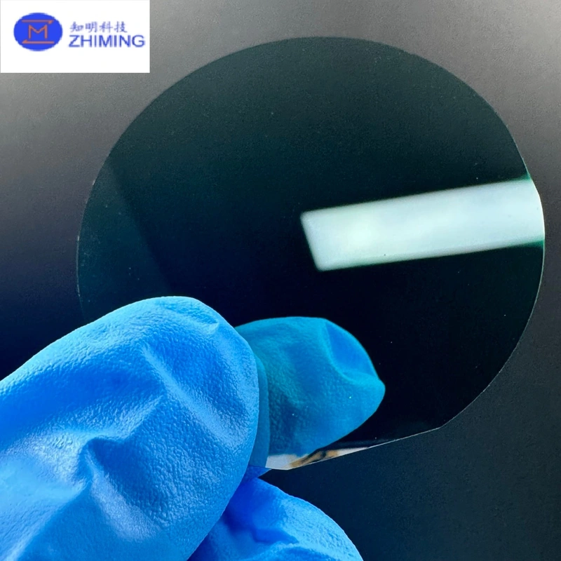
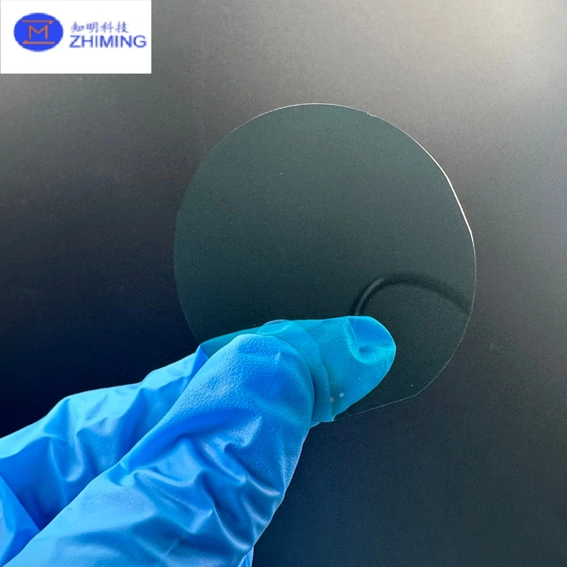
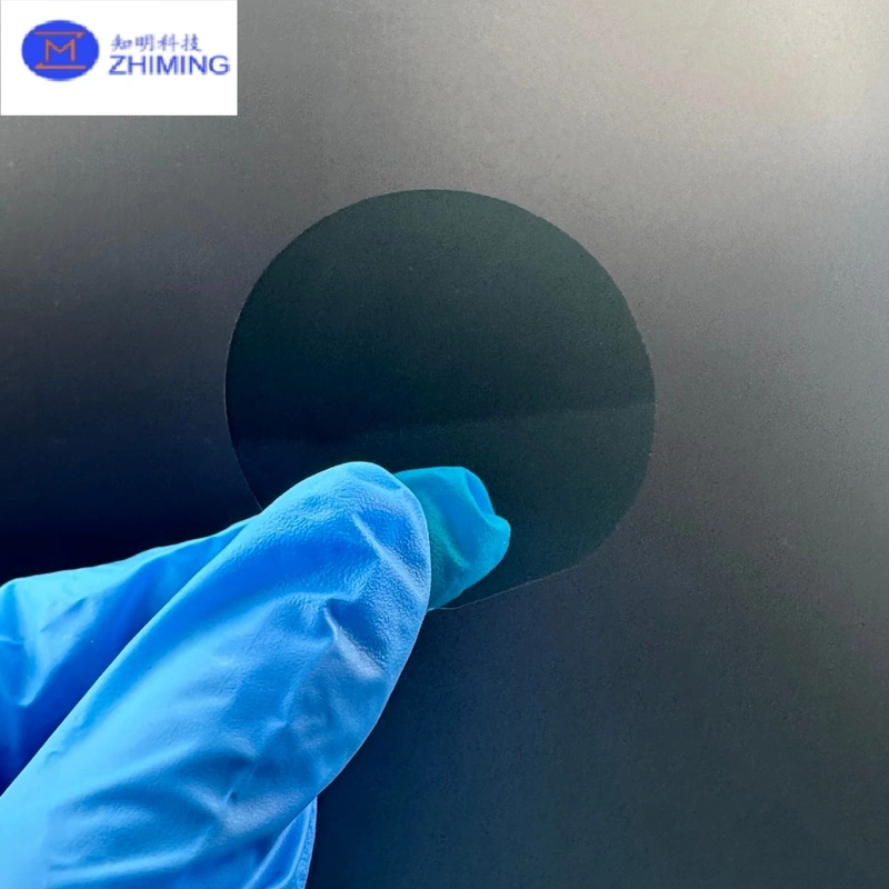
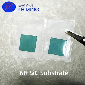
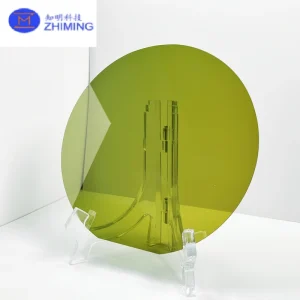
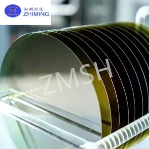
 The 6H-N Type Silicon Carbide (SiC) wafer is a high-quality 2-inch single-crystal substrate designed for high-frequency, high-power, and high-temperature semiconductor applications. Available in thickness options of 350µm and 650µm, this wafer provides excellent electrical conductivity, thermal stability, and mechanical durability, making it ideal for RF devices, microwave electronics, and specialized power components.
As a wide bandgap semiconductor (≈3.02 eV), 6H-SiC enables devices to operate under extreme conditions, including high voltage, high frequency, and elevated temperatures beyond the capabilities of conventional silicon. Compared to traditional materials, SiC significantly reduces switching losses, thermal stress, and system size, making it a key material in next-generation electronics.
Key Features
1. High-Quality 6H Polytype Structure
This wafer is manufactured using advanced Physical Vapor Transport (PVT) crystal growth technology, ensuring a stable 6H-SiC crystal structure. Compared with 4H-SiC, the 6H polytype offers advantages in RF and microwave applications, providing reliable performance in high-frequency environments.
2. Excellent Surface Quality
- Si-face CMP polishing achieves Ra < 0.2 nm, delivering an ultra-smooth, epi-ready surface.
- C-face MP finishing available for flexible processing needs.
- Minimizes surface defects and improves epitaxial layer quality, resulting in higher device yield.
3. Optimized Electrical Performance
- N-type conductivity with resistivity of 0.015–0.028 Ω·cm
- Suitable for high-power and high-frequency device fabrication
- Supports stable operation under high electric fields (3–5 × 10⁶ V/cm)
4. Superior Thermal & Mechanical Properties
- Thermal conductivity up to ~4.2 W/cm·K, enabling efficient heat dissipation
- Mohs hardness ~9.2, close to diamond, ensuring excellent wear resistance
- Maintains structural integrity at temperatures exceeding 600°C
5. Flexible Customization
We provide customization options to meet diverse application requirements:
- Thickness options (350µm / 650µm or customized)
- Surface treatments (CMP, MP, epi-ready)
- Doping and resistivity adjustments
- Wafer sizes and special coatings
Applications
High-Frequency & RF Devices
6H-SiC wafers are widely used in microwave electronics, RF amplifiers, radar systems, and satellite communication, where low signal loss and thermal stability are critical.
Power Electronics
Suitable for Schottky diodes, high-voltage rectifiers, and power modules, especially in applications requiring high efficiency and reliability.
Optoelectronics
Used in UV photodetectors, laser diodes, and optical sensors, benefiting from SiC’s wide bandgap and optical transparency.
Aerospace & Defense
Capable of operating in radiation, high-temperature, and high-stress environments, making it ideal for aerospace and military electronics.
Research & Development
Widely used in universities and industrial labs for material research, device prototyping, and process validation.
Manufacturing Highlights
- PVT Crystal Growth: Ensures high-purity single-crystal SiC with controlled defect density
- Precision Slicing: Diamond wire cutting for accurate wafer thickness
- Lapping & Grinding: Achieves excellent flatness and uniformity
- CMP Polishing: Produces mirror-like, epi-ready surfaces
- Strict Quality Control: Includes inspection of defect density, resistivity, surface roughness, and thickness
Technical Specifications
| Parameter | Specification |
|---|---|
| Material | SiC Single Crystal |
| Diameter | 2 inch |
| Thickness | 350µm / 650µm |
| Polytype | 6H-N |
| Resistivity | 0.015–0.028 Ω·cm |
| Surface Finish | Si-face CMP, C-face MP |
| Surface Roughness | Ra < 0.2 nm |
| Color | Transparent |
| Packaging | Single wafer container |
Customization Options
- Thickness Adjustment: Tailored to your device structure
- Surface Processing: DSP, CMP, or epi-ready
- Doping Control: Custom resistivity ranges available
- Special Coatings: Optical or protective coatings upon request
FAQs
Q1: What is the advantage of 6H-SiC compared to 4H-SiC?
A: 6H-SiC is more suitable for RF and microwave applications, offering stable performance in high-frequency environments, while 4H-SiC is typically preferred for high-power MOSFET devices.
Q2: Are these wafers epi-ready?
A: Yes, the Si-face is CMP polished to epi-ready standards, allowing direct epitaxial growth.
Q3: Can I customize resistivity and thickness?
A: Yes, we provide flexible customization based on your device requirements.
Q4: How does SiC perform under extreme conditions?
A: SiC maintains excellent electrical and mechanical stability above 600°C, making it ideal for harsh environments.
Reviews
There are no reviews yet.