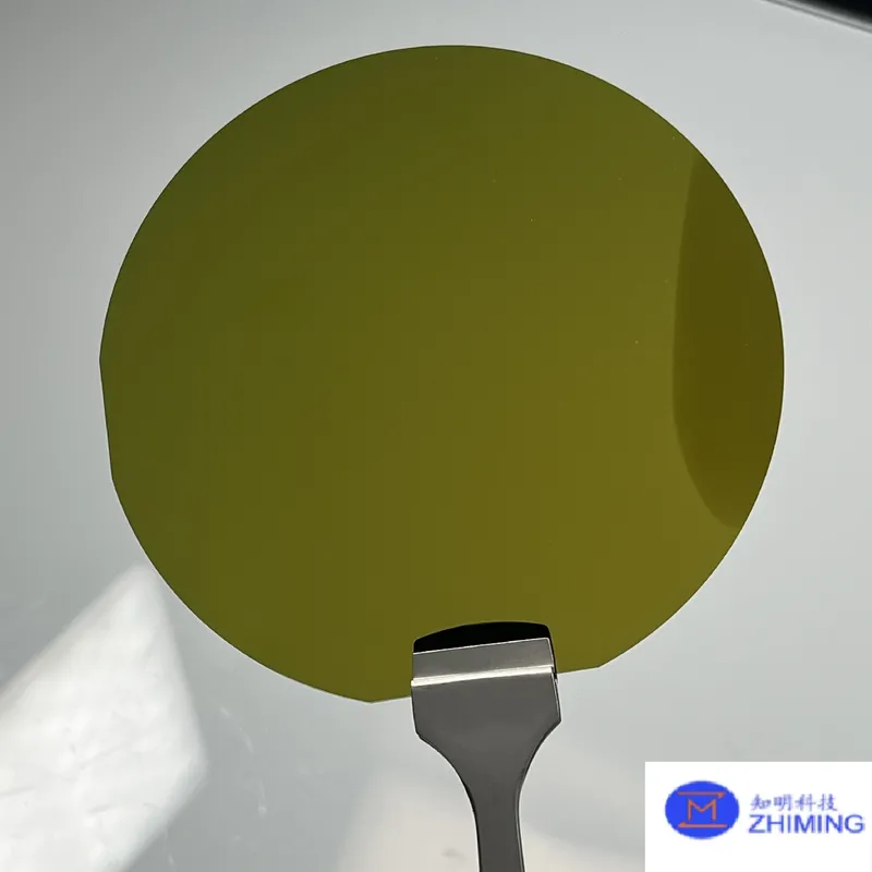
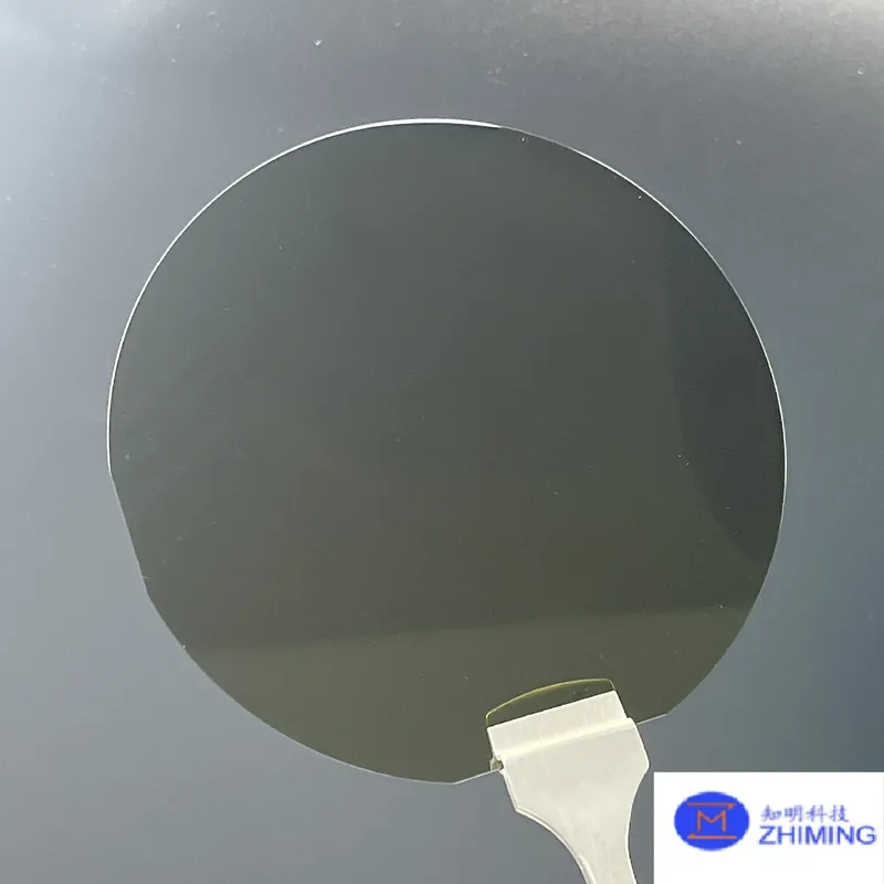

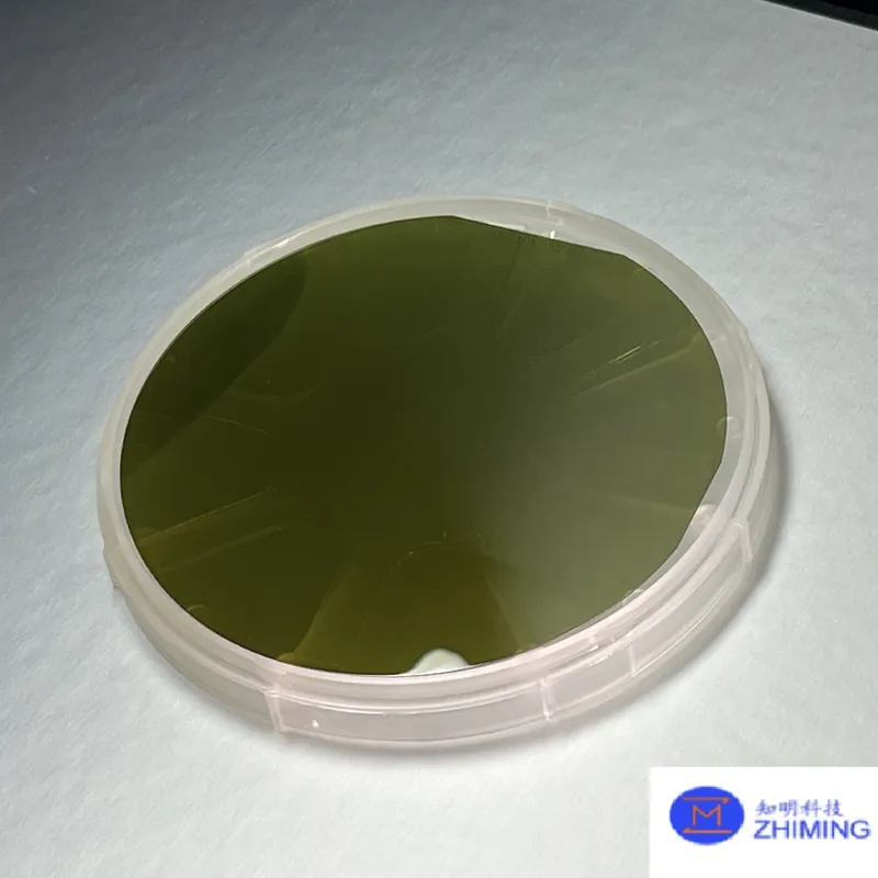
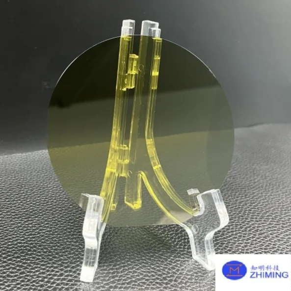
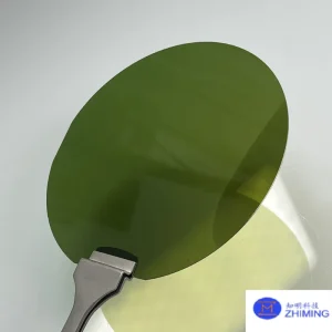
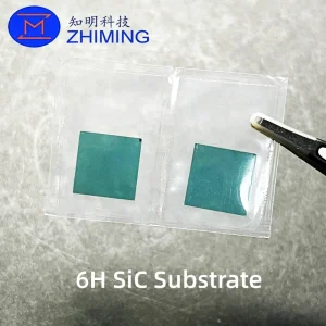
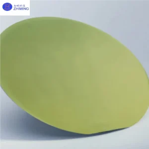
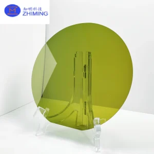
 Our 4-inch, 350µm ±25µm 4H-N Silicon Carbide (SiC) wafers are engineered for the most demanding applications in power electronics, renewable energy, electric vehicles (EVs), and industrial high-frequency devices. Featuring a 4° ±0.5° off-cut toward the <11-20> plane and N-type conductivity, these wafers deliver unmatched performance in high-voltage, high-frequency, and high-temperature environments. As a third-generation semiconductor material, SiC is revolutionizing power devices by offering a threefold increase in bandgap energy and a tenfold increase in breakdown electric field strength compared to traditional silicon, enabling smaller, lighter, and more efficient devices.
Key Features and Advantages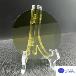
- High-Quality 4H Polytype Structure
The wafers are grown using advanced Physical Vapor Transport (PVT) technology to achieve high-purity 4H-SiC crystals. This ensures maximum electron mobility and superior thermal conductivity, which are critical for high-efficiency MOSFETs and Schottky devices. Our defect-blocking growth process prevents basal plane dislocations (BPDs) from migrating to the epitaxial surface, providing long-term device reliability. - Superior Surface Finish
Each wafer undergoes state-of-the-art Chemical Mechanical Polishing (CMP), producing an atomically flat, epi-ready Si-face (0001) with sub-nanometer surface roughness (Ra <0.2nm). This eliminates sub-surface damage and ensures a smooth surface for epitaxial layer growth, improving device yields for production-grade MOSFETs and diodes. - Multiple Grades for Different Applications
- Prime Grade (P): Optimized for mass production with lowest micropipe density (MPD ≤ 0.2 cm¯²). Ideal for EV traction inverters, solar string inverters, and high-performance industrial modules.
- Research Grade (R): Cost-effective option for R&D, university labs, and process testing. Maintains 4H structural integrity while tolerating slightly higher defect densities.
- Dummy Grade (D): Suitable for equipment calibration, polishing trials, or non-critical applications.
- Versatile Customization
We provide tailored wafer thicknesses, off-cut angles (standard 4° or on-axis), and doping levels. Our wafers support N-type conductivity for EV power modules or semi-insulating structures for high-frequency RF applications, enabling consistent electrical performance across various device types.
 Applications
- Electric Vehicles and E-Mobility: SiC MOSFETs replace traditional Silicon IGBTs in traction inverters, delivering >99% DC-to-AC conversion efficiency, reducing energy loss, and allowing more compact and lighter inverter designs.
- Renewable Energy and Smart Grids: SiC wafers enable high-frequency inverter operation, reducing the size of expensive passive components like inductors and capacitors by up to 50%. This improves system efficiency and lowers costs.
- Industrial High-Power Modules: SiC devices excel in environments requiring high-voltage handling, thermal stability, and long-term reliability, including EV charging stations, robotics, and factory automation systems.
- Rail and High-Speed Traction: SiC modules for locomotives and high-speed trains allow up to 30% weight reduction while operating more quietly.
- 5G & RF Electronics: High-purity, low-defect N-type SiC wafers are ideal for high-frequency, high-power RF devices, improving signal integrity and thermal management.
Manufacturing Highlights
- High-Stability PVT Growth ensures consistent 4H polytype quality and minimal structural defects.
- Defect-Blocking Mechanism prevents basal plane dislocations from affecting device layers, enhancing long-term reliability.
- Epi-Ready Surfaces remove sub-surface damage and microscopic scratches, saving time in downstream epitaxial growth processes.
- Quality Control includes precise measurements of thickness, diameter, orientation, and surface roughness, ensuring uniformity across batches.
Technical Specifications
| Parameter | Specification |
|---|---|
| Material | Monocrystalline SiC |
| Diameter | 4 inch / 101.6 mm |
| Thickness | 350µm ±25µm |
| Polytype | 4H-N |
| Surface Finish | DSP, CMP/MP |
| Off-Cut Angle | 4° toward <11-20> ±0.5° |
| Packaging | Cassette box or single wafer container |
| Applications | EV inverters, power electronics, renewable energy, 5G RF |
FAQ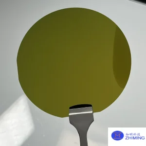
Q1: Does Research Grade mean defective?
A1: No. R-grade wafers maintain 4H-SiC integrity but may have higher micropipe density. Ideal for R&D or non-critical processes.
Q2: Why is SiC more expensive than Silicon?
A2: SiC takes ~2 weeks to grow using specialized PVT techniques, and its hardness near diamond requires diamond-tipped tools for slicing and polishing. This results in higher cost but unparalleled performance under high voltage and temperature.
Q3: Do epi-ready wafers require additional polishing?
A3: No. Epi-ready wafers are polished to atomic smoothness and ready for epitaxial growth. MP or dummy wafers may require additional polishing.
Reviews
There are no reviews yet.