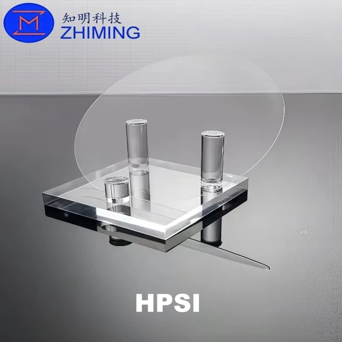
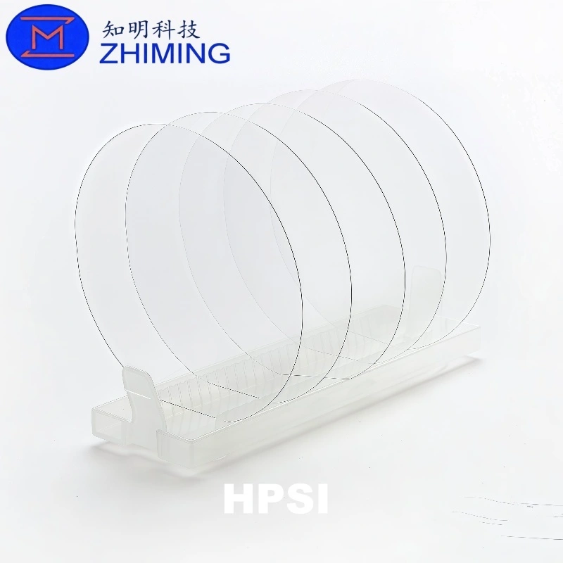
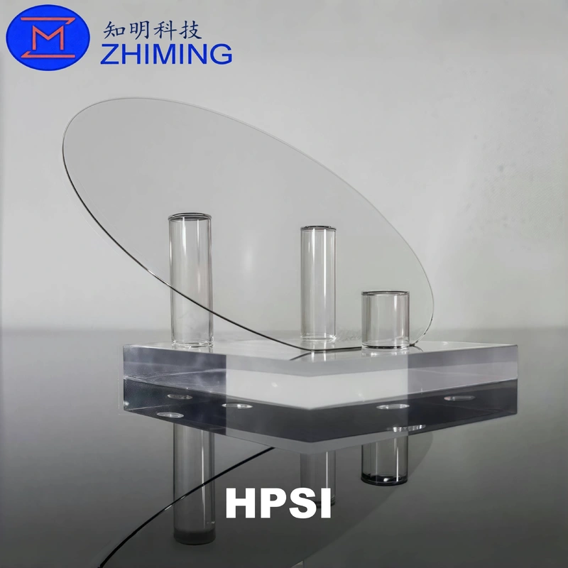
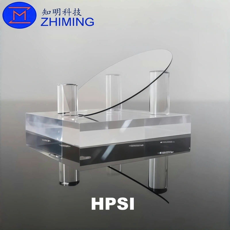
HPSI (High-Purity Semi-Insulating) Silicon Carbide wafers are advanced wide bandgap semiconductor substrates designed for high-frequency, high-power, and optical applications. Based on 4H-SiC polytype, these wafers offer ultra-high resistivity, excellent thermal conductivity, and superior optical performance.
They are widely used in AR/AI optical systems, RF devices, and next-generation photonics, especially for waveguide optics in AR glasses.
Key Features & Advantages
 1. Ultra-High Purity & Semi-Insulating Performance
- Resistivity up to ≥1E10 Ω·cm
- Ideal for RF, microwave, and photonic devices
- Minimizes parasitic capacitance and signal loss
2. Excellent Optical Properties
- Refractive Index: 2.6 – 2.7 (400–800 nm)
- Low optical absorption
- Eliminates rainbow effect in AR waveguides
- Enables single-layer optical design
3. Outstanding Thermal Conductivity
- Thermal Conductivity: ~490 W/m·K
- Efficient heat dissipation for Micro-LED & laser systems
- Ensures stability under high power operation
4. Superior Mechanical Strength
- Mohs Hardness: 9.5
- High scratch resistance
- Long service life in harsh environments
5. Semiconductor Process Compatibility
- Compatible with CMOS processes
- Supports nano-scale lithography & etching
- Enables wafer-level fabrication of optical components
Technical Specifications
| Parameter | Specification |
|---|---|
| Material | HPSI 4H-SiC |
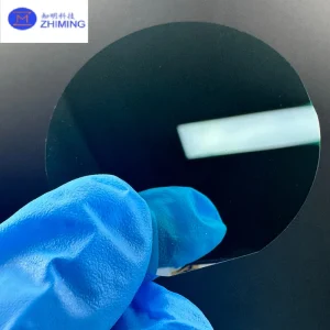
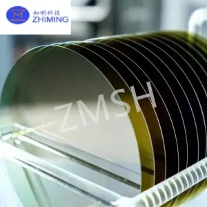
| Diameter | 2″, 3″, 4″, 6″, 8″ |
| Thickness | 500 ± 25 μm |
| Resistivity | ≥1E5 – ≥1E10 Ω·cm |
| TTV | ≤5 / ≤10 / ≤15 μm |
| Bow | ±25 / ±35 / ±45 μm |
| Warp | ≤35 / ≤45 / ≤55 μm |
| Surface | CMP Polished (Ra ≤0.2 nm) |
| Grade | Prime / Dummy / Research |
| Certification | RoHS |
Core Applications
1. AR / AI Optical Systems
- Waveguide lenses (diffractive optics)
- Micro-display optical coupling
- Anti-reflective optical substrates
Enables:
- Wider FOV (70°–80%)
- Ultra-thin lenses (~0.5 mm)
- High light efficiency (>80%)
2. RF & Microwave Devices
- RF substrates
- High-frequency communication components
- 5G / 6G systems
3. Advanced Photonics & Quantum Applications
- Quantum communication devices
- Color center photonics
- Integrated optical chips
4. High-Power Laser Systems
- Laser diode substrates
- Industrial & medical laser components
Why Choose ZMSH?
✔ Vertical Integration
- In-house crystal growth (2″–12″)
- Full control over purity & defects
✔ Precision Processing
- CMP polishing: Ra < 0.3 nm
- Laser dicing & custom shaping
- Optical-grade finishing available
✔ Customization Capability
- Doping control
- Thickness & orientation customization
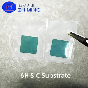
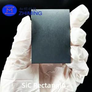
- Custom shapes: prism, square, waveguide arrays
✔ B2B Full-Service Support
- Sample supply
- Technical consultation
- Mass production support
FAQ
Q1: Why is HPSI SiC ideal for AR optics?
HPSI SiC provides high refractive index and low absorption, enabling thinner waveguides and eliminating chromatic distortion.
Q2: What is the difference between HPSI SiC and conductive SiC?
HPSI SiC is semi-insulating with very high resistivity, mainly used for RF and optical applications, while conductive SiC is used in power electronics.
Q3: Can you support custom specifications?
Yes, we support customization in size, thickness, resistivity, and surface finish.
Reviews
There are no reviews yet.