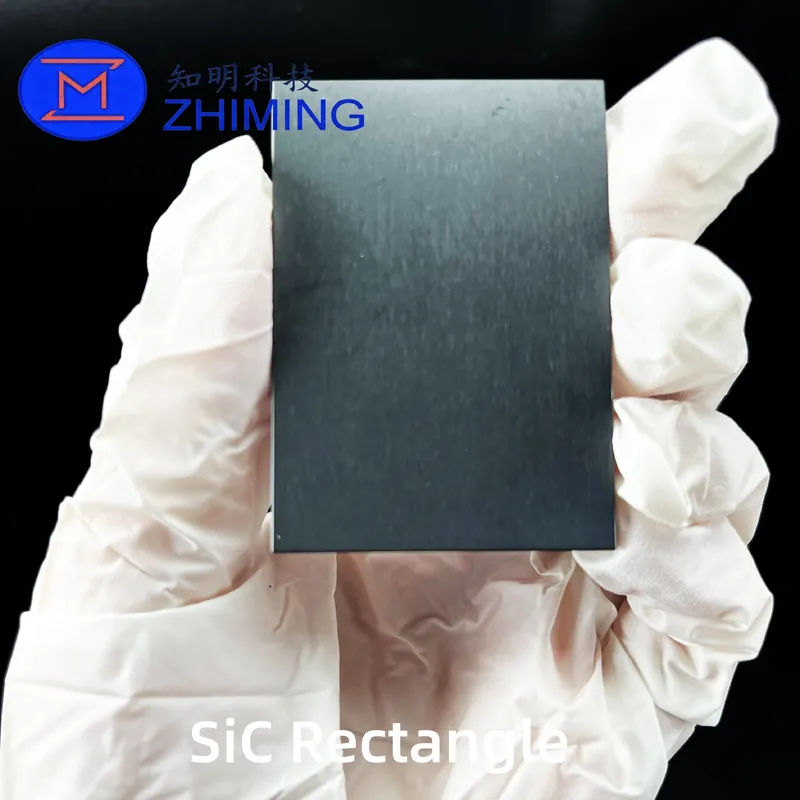
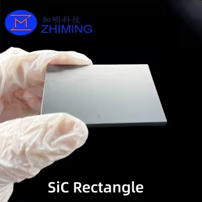

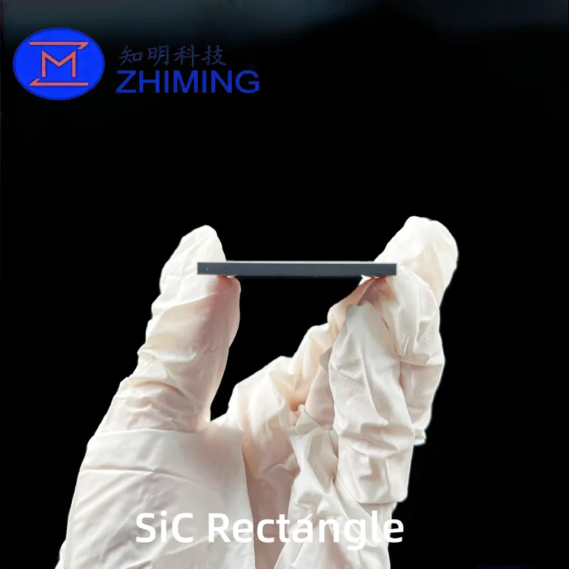
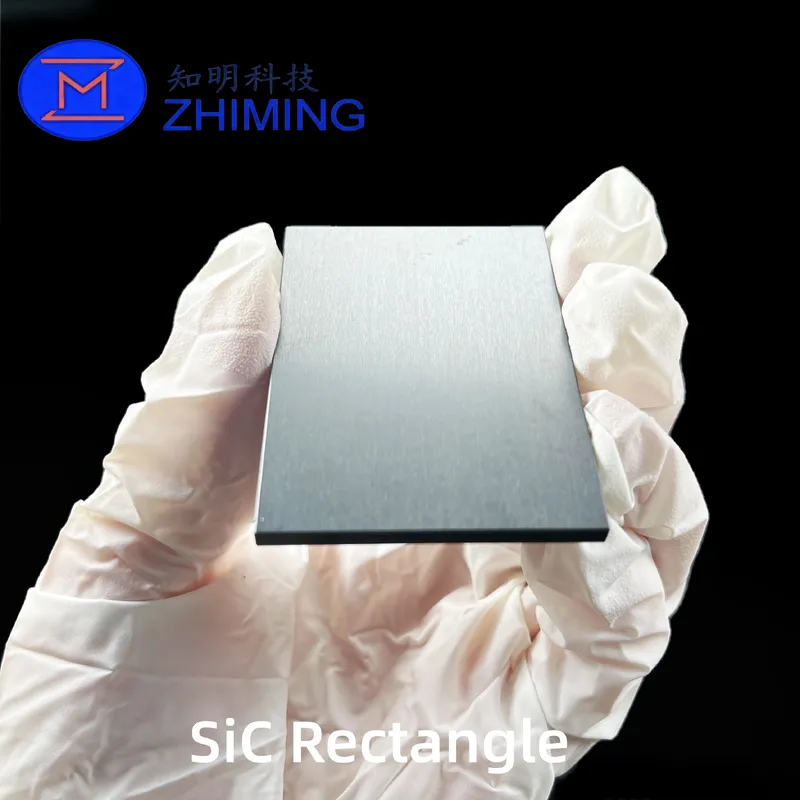
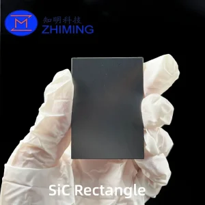
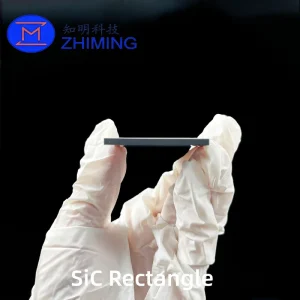
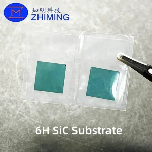
The Silicon Carbide (SiC) rectangle substrate is a high-performance single-crystal semiconductor designed for advanced power electronics, RF/microwave devices, optoelectronic components, and extreme-environment applications. Available in custom rectangular sizes with thickness ranging from 330–500 μm, these SiC substrates are manufactured in 4H or 6H polytypes and are suitable for both N-type and P-type doping.
SiC is distinguished by its wide bandgap (3.2–3.3 eV), high thermal conductivity (3.0–4.9 W/cm·K), and exceptional mechanical strength (Mohs hardness ~9.2), enabling devices that operate reliably under high temperatures, high voltages, and high switching frequencies. Our rectangular SiC substrates are commonly used in R&D labs, prototype development, and specialized industrial applications, where precision, reliability, and performance are critical.

Key Features
- High-Purity Polytype Options
- 4H-SiC: Optimized for high-voltage power electronics, including MOSFETs and Schottky diodes, with superior electron mobility and thermal performance.
- 6H-SiC: Suited for RF, microwave, and high-frequency applications, minimizing power loss and improving signal stability.
- Advanced Surface Preparation

- Available as single- or double-side polished (DSP), with epi-ready surfaces for direct epitaxial growth.
- Sub-nanometer surface roughness ensures consistent electrical performance and high device yield.
- Flexible Doping Options
- Custom N-type or P-type doping available to meet electrical and device-specific requirements.
- Multiple Quality Grades
- Research Grade: Cost-effective for academic labs, R&D, and process testing.
- Device Grade: High-quality substrates suitable for commercial and industrial power electronics production.
- Customizable Dimensions
- Supports a wide range of rectangular sizes to match your process requirements.
- Off-axis angles of 0° or 4° toward the C-plane are available to optimize epitaxial growth and device performance.
Applications
- Power Electronics: Ideal for MOSFETs, IGBTs, and Schottky diodes used in electric vehicle inverters, energy storage systems, and industrial power conversion.
- High-Frequency & RF Devices: Perfect for radar, satellite communications, 5G base stations, and microwave applications requiring low power loss and high signal integrity.
- Optoelectronics: UV LEDs, laser diodes, and photodetectors benefit from SiC’s excellent UV transparency and thermal stability.
- Aerospace & Defense: Substrates perform reliably in radiation-prone, high-temperature, and high-stress environments.
- Academic & Industrial Research: Supports prototyping, testing, and advanced material development.
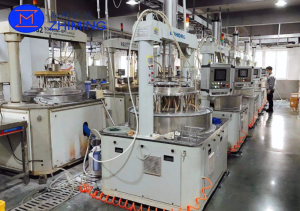 Manufacturing Highlights
- Physical Vapor Transport (PVT) Growth ensures high-purity single-crystal SiC with minimal structural defects.
- Ingot Slicing & Planarization: Diamond wire saws and lapping ensure uniform thickness and flatness.
- Chemical Mechanical Polishing (CMP): Produces mirror-smooth epi-ready surfaces, eliminating sub-surface damage.
- Quality Assurance: Rigorous testing of thickness, flatness, and defect density guarantees compliance with semiconductor standards.
Technical Specifications
| Property | Specification |
|---|---|
| Dimensions | Custom rectangular sizes |
| Thickness | 330–500 μm (customizable) |
| Polytype | 4H-SiC or 6H-SiC |
| Orientation | C-plane, off-axis 0°/4° |
| Surface Finish | Single/double-side polished, epi-ready |
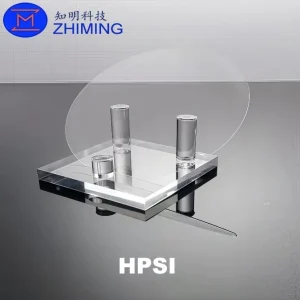
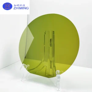
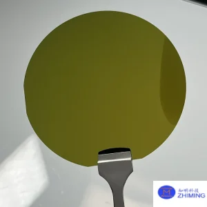
| Doping Options | N-type, P-type |
| Quality Grade | Research or Device-grade |
Customization Options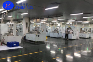
- Dimensions & Shapes: Tailored rectangular formats to match device requirements.
- Doping Profiles: N-type or P-type doping for optimized electrical performance.
- Surface Treatments: Single-side or double-side polishing; epi-ready surfaces for direct epitaxial growth.
- Packaging Solutions: Custom packaging to ensure safe delivery and minimize wafer damage.
FAQs
Q1: Why choose SiC substrates over silicon?
A1: SiC offers superior thermal performance, higher breakdown strength, and lower switching losses, making it ideal for high-efficiency, high-power applications.
Q2: Are epi-ready wafers available?
A2: Yes, we provide epi-ready surfaces suitable for high-power, RF, and optoelectronic device applications.
Q3: Can dimensions and doping be customized?
A3: Absolutely. Custom sizes, doping profiles, and surface treatments are available to meet specific application needs.
Q4: How does SiC perform under extreme conditions?
A4: SiC maintains structural integrity and electrical stability at temperatures over 600°C, suitable for aerospace, defense, and high-power industrial applications.
Reviews
There are no reviews yet.